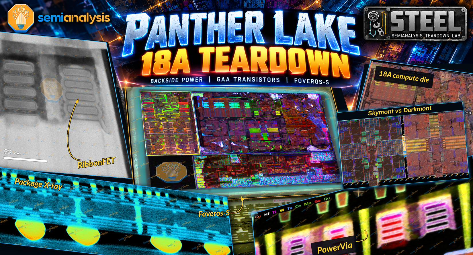
Panther Lake debuts the first commercial implementation of backside power delivery (BSPDN), introduces Intel’s first iteration of gate-all-around (GAA) transistors, and showcases their advanced packaging capabilities with its Foveros-S assembly. With Panther Lake, Intel’s manufacturing arc has shifted from nebulous roadmaps to shipped silicon, a significant milestone on their long road back to competitive semiconductor manufacturing. To evaluate the extent of Intel’s comeback, we tore down Panther Lake.
The SemiAnalysis STEEL teardown lab breaks down advanced datacenter and AI hardware. To learn more about our pipeline or to commission a teardown, contact sales@semianalysis.com.
WE’RE HIRING: Architecture, floorplan, packaging, manufacturing, and labs experts. Opportunities from system to transistor and everywhere in between. Check out our Careers page.
Our teardown traces 18A from its four-sheet RibbonFETs (Intel’s marketing name for GAAFETs) and gate stacks through contacts, frontside and backside wiring, and the bonded carrier. We explain how these material and integration choices improve gate control and reduce resistance, while adding capacitance, thermal resistance, and process complexity. Our measurements put Panther Lake’s 18A compute logic and TSMC N3E GPU logic at similar logic density. However, 18A does not lead TSMC N3P, N2 or Samsung SF2 in peak density. Panther Lake’s CPU cores are incremental updates, and the high-end GPU still uses TSMC N3E.
Panther Lake assembles one compute tile, one GPU tile, and one I/O tile atop a passive base tile using Intel’s Foveros-S advanced packaging. Both compute tile variants use Intel 18A. The Xe3 GPU options are a 4-core GT1 tile on Intel 3 and a larger 12-core GT2 tile on TSMC N3E. Both I/O tile variants use TSMC N6. [1], [2]
Our analysis centers on the PTL-U compute tile, both the 4-core and 12-core GPU tiles, as well as the 12-lane I/O tile.
In conventional chips, power and signal are routed through the same frontside metal stack towards the device frontend. Power rails consume scarce routing resources near the transistors, while tall via stacks carry VDD and VSS from the coarse upper wires to local rails. Backside power delivery (BSPD) moves the main power network behind the transistor layer, to the backside, separating it from frontside signal routing. We covered BSPD and its impacts in 2024. [3], [4], [5] Intel’s BSPD implementation, branded as “PowerVia”, routes power through dedicated backside metals to nano-TSVs, which connect those rails to local source/drain (S/D) contacts.
Implementing that separation requires Intel to build the interconnect stacks from both sides of the wafer. The frontside comprises the M0-M14 signal stack, while the backside comprises the BM0-BM5 power stack. M0 and BM0 are closest to the transistors.
The nano-TSVs connect the two sides, but Intel patterns and etches each via from the front after forming the contacts. A narrow via runs from the side of the contact deep into the silicon substrate. Intel then completes the frontside signal metal stack, bonds the wafer to a carrier, flips it and removes the original substrate until the buried via tips are exposed. The backside metal stack is then deposited directly on the revealed vias.
The nano-TSV and backside-via profiles taper in opposite directions because Intel forms them from opposite sides of the wafer. The transistor structures form the FEOL. Local contacts and nano-TSVs connect them to the wiring. M0 begins the frontside interconnect stack.
The silicon carrier remains attached above the frontside interconnects. It supports the device wafer during substrate removal and backside processing and remains part of the finished chip’s thermal path.
PowerVia removes the main power distribution from the congested frontside metals, routing supply through shorter and wider backside wires. Its lateral landing still occupies area in the standard cell, so it recovers less cell area than a direct backside contact. [3] Nano-TSVs beside the logic devices carry VDD or VSS from the backside power network, while signal connections continue upward through the frontside metals.
Backside Interconnects
Samsung SF2 data is included for comparison to Panther Lake’s within this article. SF2 is the incumbent GAA foundry node but lacks BSPD, serving as a useful reference to evaluate 18A. A full teardown of Samsung’s S26 products, processed on SF2, will be shared soon.Nanosheet-cut EDS comparison.
The PowerVia supply path runs from the backside Cu rails through Mo-lined W nano-TSVs to the local transistor contacts. In this cross section, the tapered connection spans roughly 150 nm from the contact level to BM0. The Ta liner confines Cu and promotes adhesion to the surrounding stack; the AlOₓ etch stop controls the next dielectric etch above the rail. Dielectric beneath the ribbons electrically separates the devices from the backside wiring and removes the conducting silicon body below the channel. [6]
AlOₓ serves as an etchstop (ES), enabling endpointing and protecting the underlying layers. Low-volatility aluminum fluoride reaction products resist the fluorinated plasma, allowing a thin AlOₓ film to protect the metal while the surrounding low-k dielectric is removed. [6], [7]. While the BM0 and layers above the M1 lines show double AlOx layers, Our SMIC N+3 teardown showed single AlOₓ layers. SMIC uses a simpler local AlOₓ substack, while the remaining cap and etch sequence provide the required landing protection.
So why double layers? The closely spaced AlOₓ doublets provide two protected endpoints in the etch sequence. Intel documents an AlOₓ/SiN/AlOₓ stack that explains the benefit. The main dielectric plasma etch stops on the first AlOₓ film; a selective wet clear opens that film; a second plasma etch removes the intermediate SiN and stops on the second AlOₓ film. The final wet clear exposes the metal landing surface. SiN is the intermediate dielectric in Intel’s published example. [8]
The second stop protects the metal through a cap breakthrough. Wide openings can etch faster than narrow ones, and etch depth varies across the wafer. Metal under an early-clearing opening would otherwise be exposed while other openings still need more etching. Staged protection widens the process window and reduces metal erosion, corrosion and void formation. [8]
TSMC documents AlN/AlOₓ/SiOC/AlOₓ above Cu, with AlN blocking Cu diffusion, and a simpler AlN/SiOC/AlOₓ variant that omits one AlOx film. [9] Levels with different opening sizes, aspect ratios, pattern densities and cap materials need different etch margins. A double AlOx stop is useful where another protected endpoint justifies the added processing.
The extra film adds formation, selective opening and cleaning steps, plus another set of interfaces to control adhesion, moisture, and stress. These blanket films are opened through the existing via pattern, so each film does not require another lithography mask. AlOₓ adds parasitic capacitance when it replaces lower-k dielectric; two thin AlOₓ films can nevertheless contain less AlOₓ than one thick film. Total thickness, placement, and theintermediate dielectric determine the electrical cost. Deposition chemistry also changes AlOx permittivity and residual hydroxyl content, which can oxidize the underlying metal. [7], [8], [10], [11]
The backside stack separates into relatively fine BM0-BM2 wiring near the devices and coarser BM3-BM5 power distribution. The largest pitch increase occurs between BM2 and BM3. BM0’s pitch closely matches the logic-row height, fitting local power delivery to the cell rows. Higher levels aggregate current through larger conductors: routing density becomes less important than low resistance and current capacity as the network approaches the package. This hierarchy provides wide power wiring for the power delivery network without consuming scarce frontside signal-routing resources. [3]
The SemiAnalysis STEEL teardown lab breaks down advanced datacenter and AI hardware. To learn more about our pipeline or to commission a teardown, contact sales@semianalysis.com.
WE’RE HIRING: Architecture, floorplan, packaging, manufacturing, and labs experts. Opportunities from system to transistor and everywhere in between. Check out our Careers page.
Frontside Interconnects
Intel 18A combines Mo-lined W contacts and nano-TSVs with a separate backside Cu power network. Samsung SF2 keeps power on the frontside, using Ti-based contact interfaces and Ta-based barriers and Co liners around Cu wiring.
In 18A standard-cell rows, backside power rails supply the devices through nano-TSVs within the cells, freeing frontside routing resources. Samsung’s M0 accommodates both power and signal connections.
From the device toward M0, the connection runs through a Ti-based S/D interface, W contact fill, a Mo-lined W via, and the Cu M0 wire. Mo supplies a conductive nucleation and adhesion layer for W, replacing the resistive TiN liner used in conventional W integration. This increases the effective conduction volume within the feature while retaining W fill and its established polishing, cleaning and etching processes. Intel’s Mo/W patent describes this integration tradeoff. The nano-TSV uses the same Mo-lined W construction in the backside supply path. [12]
The move from TiN to Mo is an incremental change. While a full Co or Mo fill can also reduce the volume lost to liners in very small features, it requires new integration schemes that increase complexity and risk. Cu remains attractive for wider wires due to its low resistance. As wires and vias shrink, the diffusion barrier consumes an increasing fraction of their cross-section. [12], [12], [14]
Intel uses Co/Ru liners at M0-M1, Co at M2-M4, and Nb at M5-M9. The lower-level liners help Cu adhere and reduce void formation during trench fills. Applied Materials’ Endura has new thermal control that facilitate wetting process, so the thin film continuity is good enough that good capillary pressure will drive Cu atoms to the via bottom without voiding.
Intel’s choice to use Nb is particularly interesting. Intel’s Nb patent describes a conductive diffusion barrier intended to reduce the barrier’s contribution to resistance relative to conventional Ta-based barriers, particularly at via bottoms where all current crosses the barrier. The patent pairs Nb in coarser levels with the option of lower-cost PVD processing. [15], [16]
The upper metal layers support thicker barriers formed through physical vapor deposition (PVD) despite its worse coverage and uniformity. Meanwhile, the lower metal layers require thinner barriers deposited through conformal atomic layer deposition (ALD). Co/Ru adds another material interface and requires controlled deposition and Cu fill. Changing liners and barriers by metal layer allows Intel to optimize interconnect resistance, process complexity, and reliability. [15, 16]
RibbonFET, Intel’s name for its gate-all-around FETs (GAAFETs), replaces the FinFET’s vertical fins with four stacked horizontal silicon nanosheets, allowing the gate to surround the channel on every side. The path to GAAFET begins with the planar transistor.
A planar MOSFET places the gate above the channel between its source and drain. Pairing an NMOS with a PMOS transistor creates a CMOS inverter, in which the NMOS pulls the output low for a high input, and the PMOS pulls it high for a low input. The gate must retain electrostatic control of the channel to ensure clean switching. As gate lengths shrank, the drain began to compete with the gate for that control, increasing off-state leakage.
Electrostatic control was restored through an architectural evolution that raised the channel into a vertical fin and wrapping the gate around three sides. Called “FinFET”, this new architecture packed more effective channel width into a smaller footprint. Further scaling made it harder to maintain both drive current and leakage within smaller cells, and reintroduced the same problems planar MOSFETs faced. Nanosheet GAAFETs close the fourth side by replacing the vertical fin with a stack of horizontal nanosheets, each surrounded by the gate. The tighter electrostatic control suppresses leakage at shorter gate lengths while stacking adds effective channel width within the cell footprint.
In a FinFET process, channel width changes in discrete steps as designers must add or remove whole fins. Nanosheet width can instead be adjusted continuously within the process’s design rules. Wider sheets increase drive current, while narrower sheets reduce capacitance at the cost of drive current. Intel 18A uses stacks of four nanosheets each and varies their widths across logic and SRAM. At the process level, adding more sheets to each stack increases effective channel width and drive current, but complicates fabrication.
RibbonFET vs MBCFET
Samsung began GAAFET production in 2022 with SF3E, following with SF3 and now SF2. Its ‘MBCFET’ provides a useful structural comparison with Intel’s first RibbonFET implementation. [17] STEEL is digging deeper into SF2, used in the Exynos 2600, and TSMC’s GAAFET N2, used in Apple’s A20 Pro, in upcoming newsletter articles. We’re throwing some teasers on X. Let’s compare Samsung SF2’s MBCFET with Intel 18A’s RibbonFET.
Even to the untrained eye, Intel’s extra nanosheet is obvious. Intel stacks four ribbons to Samsung’s three. Samsung’s sheets are much wider in these fields, so both sheet count and width matter to the available channel perimeter. Sheet width also changes which silicon surfaces carry current. On conventional (001) silicon, wide nanosheets emphasize the broad top and bottom surfaces, favoring electron transport; the larger sidewall contribution in a narrow sheet favors hole transport. Thinner sheets improve gate control but increase confinement and scattering. This makes width and thickness part of the NMOS/PMOS balance, alongside strain and threshold voltage. [18], [19]
GAAFET designs like 18A use different work-function-metal (WFM) stacks for NMOS and PMOS. Around each ribbon, a thin SiOx interfacial layer separates the silicon channel from the HfOx high-k dielectric, with La providing dipole tuning and the WFM wrapping the dielectric. NMOS uses a TiAl-based stack, while PMOS uses TiN WFM. W fills the remaining gate trench, providing a lower-resistivity path where the work-function layers are no longer needed. In this field, the PMOS stacks leave room for W between ribbons, while the NMOS stacks occupy more of those gaps. A silicon-based dielectric marks the P/N boundary, allowing the PMOS and NMOS gates, sharing the same gate trench, to be processed sequentially.
Fast logic paths, retention circuits, and SRAM need a family of threshold options. Changing threshold without substantially changing device dimensions, capacitance or fabrication complexity is valuable. FinFET processes typically use different work-function-metal stacks. In a four-ribbon GAA stack, the narrow sheet-to-sheet gap limits how much WFM can fit around each channel. La in the gate dielectric creates interfacial dipoles at the SiOx/HfOx boundary, shifting effective work function and tuning threshold voltage. This gives Intel another control alongside its NMOS and PMOS WFM stacks. Low-threshold devices improve critical-path drive; higher thresholds reduce leakage elsewhere. Dipole tuning is especially useful in GAA because it changes threshold without consuming the narrow intersheet gap with thicker WFM.
Precise control of La incorporation, diffusion and interface quality has long been a challenge, limiting viability in high volume production but is now seen from every leading-edge foundry. Intel’s patent describes depositing a dipole-forming oxide above HfOx and annealing it toward the interfacial oxide before completing the work-function and fill metals. This separates threshold tuning from the space available for metal. Newer research addresses the thermal cost: imec’s 2026 dipole-middle research inserts the shifter between two HfOx depositions, shortening the diffusion path while protecting SiOx during patterning. [20], [21]Matched-cut EDS, Intel 18A (left) vs. Samsung SF2 (right).
Intel retains raised source/drain epi beneath its contacts, while Samsung recesses W deep into the epi to form a V-shaped Ti-lined interface. The deeper contact increases metal-to-semiconductor area and shortens the current path from the lower sheets, reducing contact and spreading resistance. It also removes epi volume and brings the contact etch closer to the channel ends. Retaining more epi preserves the material available for strain transfer, especially from SiGe into PMOS. These geometries balance contact access against stress engineering and etch margin. [22], [23]
Samsung stacks three sheets to Intel’s four ribbons, and both processes use sheet width to tune drive strength. In our Samsung cross-sections, widths range roughly from 19 to 30 nm in the NPU rows and 37 to 50 nm in the CU cell. The Samsung nanosheets taper, with the widest sheet at the bottom and the narrowest at the top. Both processes use HfOx gate dielectric and Ti-based work-function stacks, with Al in the NMOS stack. In the Samsung devices shown here, the dielectric and WFM occupy the intersheet gaps, leaving W above the top sheet. Intel’s PMOS stack leaves more room between ribbons, and W fills those gaps while the thicker NMOS stack leaves W mainly in the upper trench. Gate-stack EDS maps.
The W between Intel’s PMOS ribbons provides a conductive path close to the lower gates. Where WFM fills the entire gap, the gate still surrounds the channel, but voltage reaches it through the more resistive work-function films. Thinner WFM and dipole tuning preserve room for low-resistivity fill; Mo and Ru are alternative fill metals being developed for further scaling. [24]
A masked, sequential WFM flow explains the different gate heights and inter-nanosheet fill. The proposed sequence below shows how separate NMOS and PMOS work-function steps produce that geometry.
Enabled by the BSPDN process, Intel replaces the dense-logic silicon subfin with dielectric, removing the parasitic conduction path below the ribbons and reducing substrate-related capacitance. A retained silicon body as in classical, non-SOI, planar and FinFET designs needs junction and punchthrough-stop engineering to suppress leakage. Dielectric isolation makes that leakage less sensitive to the subfin doping profile but adds removal and fill steps. It also weakens the direct thermal path through silicon, making the contacts, metal stacks and package more important for heat extraction. [24], [26]
Fluorine is concentrated around selected Intel device structures in the maps. WF6 is a standard precursor for W nucleation and fill, while barrier films protect adjacent dielectrics from fluorine attack. Low-fluorine W processes reduce the residual-F burden. Chloride-based precursors avoid introducing F during W deposition, but require control of chlorine attack, nucleation and fill quality. The integration target is a continuous, low-resistance W path with a thin protective liner and minimal chemical damage to the surrounding stack. [20], [27], [28]
The SemiAnalysis STEEL teardown lab breaks down advanced datacenter and AI hardware. To learn more about our pipeline or to commission a teardown, contact sales@semianalysis.com.
WE’RE HIRING: Architecture, floorplan, packaging, manufacturing, and labs experts. Opportunities from system to transistor and everywhere in between. Check out our Careers page.
We measured cell height, gate pitch, metal geometry, and ribbon dimensions at the XTEM sites shown below. The tables group these dimensions by site and device polarity. Our “sheet cuts” cross the silicon channel and show the ribbons end-on. “gate cuts” run along the channel through successive gates.
The 18A logic cell dimensions point to a five-track logic library while the N3E and Intel 3 cell dimensions evidence a seven-track logic library. The DDR-PHY uses wider M0 wires and much larger spacing than core logic. That trades routing density for lower wire resistance and weaker coupling between neighboring nets. The geometry suits the current delivery and coupling requirements of analog, clock, and I/O circuitry.
PowerVia lets 18A combine a compact cell height with wider M0 geometry by moving the main power rails off the signal-routing tracks. That relaxes local wire scaling while preserving a small cell footprint. Cell height and gate pitch set the geometric density; pin access and routability determine how much of it a real block can use. [29]
The biggest takeaway from our gate-pitch measurements is that Intel 18A compute logic and TSMC N3E GPU logic have similar density in the Bohr representative-cell model. The 18A example is 18.6% denser than the Intel 3 GPU example. Gate pitches are nearly identical across the three sites, so cell height drives most of the difference.
The Bohr model combines a four-transistor NAND2 spanning three gate pitches and a 32-transistor scan flip-flop (SFF) spanning nineteen pitches, weighting their densities 60:40. The sensitivity column shows how independently changing cell height and gate pitch by ±1 nm changes the result. This compares representative cell geometries; whole-die density also depends on cell mix and placement.
The 18A P-core gives M0 substantially more metal cross section than the N3E vector engine. Treating each profile as a trapezoid gives 2.63 times the area per line and 1.84 times the area after normalization by routing pitch. The larger section reduces the geometric contribution to line resistance and lowers current density for a given current. Taller and wider wires also add capacitance, so circuit delay depends on the balance of resistance and capacitance. The DDR-PHY has less metal area per routing width than the 18A core fields, while remaining above N3E. [30]
Area = height × (top CD + bottom CD) / 2, including liners. Area/pitch normalizes by routing width. Taper is the symmetric sidewall angle from vertical, with the largest angle belonging to the DDR-PHY.
Compute tile
The measurements show how ribbon dimensions and gate-stack geometry vary across the compute tile and between NMOS and PMOS to balance channel drive, gate load and the space needed for the dielectric/WFM stack across logic, SRAM and the DDR-PHY. Width mainly changes available channel perimeter; thickness also changes electrostatic control and carrier confinement. Gate-stack thickness then determines the space left for low-resistivity fill
P-core and LP E-core logic
Both the P-core and LP E-core use multiple nanosheet widths. Widths are measured on high-magnification XTEMs while wider-field images demonstrate additional width choices within the LP E-core. Multiple widths are expected even within an LP E-core. Timing-critical paths, buffers and cells with different fanout need different drive strengths. The lower-magnification fields show this width diversity beyond the sites quantified in the table.
L2 and L3 SRAM
GAA gives SRAM designers another way to balance the pull-up (PU), pass-gate (PG), and pull-down (PD) transistors. FinFET bitcells set device strength through fin count while GAA adds nanosheet width as a sizing knob. In a 6T SRAM cell, a strong pull-down relative to the pass-gate limits read disturbance, while a strong pass-gate relative to the pull-up improves writability. During a write, the pass-gate and write driver pull the node storing “1” below the inverter trip point. During a read, the pull-down holds the node storing “0” low. Bias, threshold voltage, mismatch and assist circuitry set the remaining margin. FinFET high-current cells commonly use a PU:PG:PD fin-count pattern of 1:2:2, a device-sizing ratio rather than a current ratio.
Ribbon width lets Intel balance SRAM strengths without adding whole fins. The L2 cell uses its narrowest ribbons for PU and widest for PD, improving writability and read stability respectively. Intel’s disclosed HCC operates without assist; its denser HDC uses negative-bitline write assist. Pulling the selected bitline briefly below ground increases pass-gate overdrive so it can overpower the pull-up at lower supply voltage. That buys density and low voltage writability at the cost of boosting circuitry, switching energy, and additional voltage stress that must be controlled. [31], [32]
Four rectangular ribbons give the perimeter = 8 × (width + thickness), before corner rounding. PG/PU is 1.49 and PD/PG is 1.16.
The L3 structures closely resemble L2 in layout and cell height. Fewer L3 nanosheet widths are tabulated because fewer high-magnification images were available.
DDR PHY
The DDR-PHY trades density for controlled analog behavior and reliable off-chip signaling. It contains drivers, receivers, delay circuits, and calibration logic that set drive strength, sampling time, and voltage margin. Repeated four-sheet devices with similar widths fit the use of regular transistor units for matching and programmable drive. Its wider local wiring provides room for current delivery and separation of sensitive signals, while consuming more area than a dense core-logic grid. The layout serves the memory channel’s electrical requirements as well as digital logic density. [33]
The SemiAnalysis STEEL teardown lab breaks down advanced datacenter and AI hardware. To learn more about our pipeline or to commission a teardown, contact sales@semianalysis.com.
WE’RE HIRING: Architecture, floorplan, packaging, manufacturing, and labs experts. Opportunities from system to transistor and everywhere in between. Check out our Careers page.
Intel 3 GPU devices
Vector engine logic
Intel 3’s XVE logic uses two-fin PMOS and NMOS devices with power rails in M0. Its cell height and M0 pitch give a seven-track geometry, two tracks more than the 18A logic. One-fin groups also appear among the two-fin devices.
Intel 3 L2 SRAM
The Intel 3 L2 SRAM uses the familiar HCC sizing pattern: one PU fin, two PG fins, and two PD fins.
N3E GPU devices
Vector engine logic
The N3E XVE field contains repeated two-fin devices with seven-track cell geometry. N3E remains a FinFET process, giving Panther Lake a direct FinFET-to-RibbonFET comparison.
N3E L2 SRAM
The N3E L2 SRAM uses the same PU:PG:PD fin-count pattern of 1:2:2.
Panther Lake-U follows Lunar Lake’s floorplan quite closely. Both pair 4 P-cores with 4 LP E-cores and NPU, media and display engines in similar locations. Lunar Lake also uses Xe2, the direct predecessor to Panther Lake’s Xe3 GPU. This makes Lunar Lake the most direct basis for our comparisons. Arrow Lake differs in core count and uses the older Xe-LPG GPU architecture, so we only use it where it offers a more direct component-level comparison.
Compute tile
Panther Lake compute-tile floorplans remain sparse even months after launch. Intel 18A’s backside metal and dielectric stack must be removed without damaging the underlying structures before a clean transistor-level floorplan can be imaged. Most published die shots hide or heavily process the background, but we are quite proud of the die shot we achieved and are excited to show the work we have done.
We measured the areas of the key components on the compute tile and compared them with their Lunar Lake predecessors on TSMC N3B. These help us to capture changes in block area and compare the two chips across process nodes and designs.
Our total tile areas exclude the scribe-line area. The compute-plus-GPU subtotal below uses the PTL-U compute tile and GT1 GPU; it excludes the I/O tile and passive base. Individual block areas use the boundaries marked on the floorplans
The compute-plus-GPU row is recomputed from the displayed PTL-U and GT1 areas. Component rows use their stated per-region counts and are not an additive partition of the whole tile.
The P-core area remains almost unchanged between Lunar Lake and Panther Lake, despite L2 capacity increasing from 2.5 MiB to 3 MiB. Arrow Lake uses the same Lion Cove core as Lunar Lake but also has a 3 MiB L2. Cougar Cove fits 20% more L2 into the same P-core area. The larger private cache keeps more of each core’s working set close to its execution units, reducing access to shared L3 and DRAM. Extra capacity adds storage leakage and lookup energy, so designers balance it against avoided lower-level accesses. The shared P-core L3 cache also shrank by 14.8%. [2]
Cougar Cove combines a similar footprint with Intel’s reported power-efficiency improvements. RibbonFET’s tighter channel control reduces leakage, while PowerVia reduces supply droop and allows tighter voltage guardbands. [1]
Darkmont’s four-core LP E-core cluster is 5.0% smaller than Skymont’s on Lunar Lake, with most of the reduction in its L2 regions. The 1 MiB region shrank by 8.4% and the 1.5 MiB region by 14.9%. The tag arrays also use one fewer visible row. Tags identify which memory addresses the data array holds, so rearranging them changes the cache’s layout and wiring without requiring less data capacity. [2]
The LP E-cores share one L2. This pools capacity and avoids duplicating all the cache machinery, but the four cores contend for its banks and bandwidth. Their separate cluster also keeps light work away from the performance cluster and its L3, allowing that larger domain to sleep. [1], [2]
Cache area includes more than the storage cells. Tags identify each line, decoders select rows, sense amplifiers read the small bitline signal, and wires connect to the banks. Splitting an array into smaller sections shortens wordlines and bitlines, improving access speed, but duplicates peripheral circuits. Panther Lake’s smaller cache regions therefore reflect the complete memory implementation, including how much of each region is devoted to storage. [34]
Unlike Meteor Lake and Arrow Lake, Panther Lake has no separate SoC tile. The NPU, LP E-cores, memory controllers, PHYs, media and display engines now share the compute tile. This removes an active die and keeps CPU memory traffic on one die. The cost is moving PHY and I/O-related circuitry onto 18A: drivers, receivers and analog circuits must still meet external voltage, loading and signal-integrity requirements, so their area does not shrink like dense digital logic. [1], [2]
The biggest shrink comes from the NPU, which occupies 36.9% less area. NPU 5 consolidates the same total INT8 MAC count into half as many neural compute engines. Each of the three NCEs has a larger MAC array to make the complete NCE envelope 22.6% larger than an NPU 4 engine. Consolidation also halves the number of scratchpads and SHAVE DSPs, from 12 to 6. The MAC array handles matrix multiplication and convolution, while SHAVE executes vector and custom operations that fit the array poorly. [1], [2], [35]
The paired floorplans identify each NCE envelope and its scratchpad, MAC, and SHAVE regions. Each measured MAC polygon is counted once per NCE in the area accounting below.
The scratchpads store weights, activations, and intermediate results near the MAC arrays, allowing repeated use without fetching them again from DRAM. Halving their number delivers the largest measured area saving but leaves less local storage for the same total MAC count. Layers that no longer fit locally require smaller working tiles or more transfers of intermediate data. The benefit depends on keeping the enlarged arrays busy while managing that tighter storage budget. [36]
NPU 5 also adds native FP8. Using half the operand width of FP16 reduces storage and transfer demand, helping workloads fit the smaller local memory budget. Lower precision and format-dependent range make scaling and model validation part of deployment. Hardware activation functions further reduce work that would otherwise occupy the programmable DSPs. [1], [2]
Microsoft requires an NPU to deliver at least 40 TOPS for Copilot+ PCs. Both Lunar Lake and Panther Lake meet this threshold, but Panther Lake uses significantly less silicon.
GPU tiles
Panther Lake is Intel’s first product with Xe3, its latest GPU architecture. It offers two different GPU tiles: a smaller GT1 tile with 4 Xe3 cores on Intel 3 and a larger GT2 tile with 12 Xe3 cores on TSMC N3E.
Panther Lake allows us to compare the same GPU architecture across both Intel 3 and TSMC N3E. Wildcat Lake adds a third Xe3 implementation on Intel 18A. A future newsletter will detail Xe3 and its implementation differences across all three process nodes.
GT2 scales Xe3 to a different physical layout, with render slices arranged vertically instead of GT1’s horizontal arrangement. Slice placement sets the distances to shared cache banks and the D2D interface. Those wires consume area and add delay, so scaling the number of Xe cores also requires a new balance of cache placement, routing and timing. [1]
What’s immediately obvious is that the GT2 tile on TSMC N3E has much smaller Xe cores than GT1. These block areas include logic, caches, and routing.
An Xe core on the GT1 tile is ~69% larger than one on Lunar Lake, and ~55% larger than one on GT2. Intel 3 therefore uses substantially more area per Xe core. The block-area gap exceeds the measured logic and SRAM density gaps, bringing routing, timing targets, cell mix, and floorplan allocation into the comparison.
The measured vector/matrix engine region is almost unchanged between Lunar Lake and Panther Lake’s GT2 tile. Xe3 retains eight 512-bit vector engines and eight 2048-bit XMX engines per core. Its gains also come from feeding those engines more effectively: more resident threads hide stalls, and variable register allocation lets shaders trade registers per thread against the number of threads kept active. [1]
The shared L1/SLM capacity increased by 33% from 192 KiB to 256 KiB, while its area increased only 5%, raising effective density by 27%. L1 retains reused cache lines, while software-managed SLM lets a thread group share data locally. Both reduce traffic to more distant memory. Allocating more SLM per group can also limit how many groups reside on a core at once. [1], [37]
The GT1 tile carries 4 MiB of L2 against 16 MiB on the GT2 tile. GT1 divides its L2 cache into four 1 MiB banks, while GT2 uses eight 2 MiB banks. Each bank contains 128 macros, but each N3E macro stores 16 KiB, twice the Intel 3 macro’s 8 KiB capacity. The N3E macro is only 54% larger while holding twice as many bits, giving it 30% higher density: ~23.7 Mbit/mm² versus 18.3 Mbit/mm². Including bank-level circuitry, the gap widens to ~16.9 Mbit/mm² on GT2 versus ~10.4 Mbit/mm² on GT1.
GT2 gains density with its macros storing more bits per unit area, and those macros occupy more of each cache bank. Larger macros spread decoder and sense-amplifier overhead across more storage, while a more compact bank layout reduces the share spent on control and routing. The compromise is longer wordlines and bitlines that carry more capacitance. [34]
I/O tile
Panther Lake uses two I/O tile variants, both fabricated on TSMC N6. The smaller one provides 4 PCIe 5.0 and 8 PCIe 4.0 lanes and serves lower-tier systems as well as those without a discrete GPU, while the larger one adds 8 PCIe 5.0 lanes, bringing the total to 20 lanes, for discrete-GPU connectivity. Panther Lake SKUs with the larger 10- or 12-Xe GPUs use the smaller I/O tile. [38]
The smaller I/O tile adds a PCIe 4.0 block and a Thunderbolt block to Lunar Lake’s I/O layout, providing four additional PCIe 4.0 lanes and another Thunderbolt 4 port. Its repeated N6 blocks retain nearly identical areas and layouts. Reusing these proven PHYs and controllers avoids porting and requalifying external interfaces on 18A, where faster digital logic offers less benefit to circuits constrained by the off-chip link. [38]
SemiAnalysis’s teardown lab (STEEL) dives deep into the world’s advanced datacenter and AI hardware. To learn more about our pipeline or to commission a teardown, contact sales@semianalysis.com.
We’re hiring technical experts from system to transistor and everywhere in between. Check out our Careers page.
Panther Lake offers scalability and modularity through its disaggregated packaging that partition compute, GPU, and I/O silicon into separate tiles allowing for a suite of tile configurations. This partitioning makes the package part of Intel’s node economics as it determines how much leading-edge wafer area each product consumes, which functions can remain on other processes, and how much configuration freedom Intel can offer from a shared set of tiles.
Furthermore, fabricating the compute and GPU tiles separately confines the new 18A process to the compute tile and allows graphics and I/O to use other, more established, and more cost-effective processes. For Panther Lake, the GPU and I/O tiles are assembled alongside the compute tile on a passive silicon base using Foveros-S.
Intel’s current technology brief lists a nominal 36 µm pitch for Foveros-S. Through-silicon vias (TSVs) in the base connect the fine wiring above to the larger package connections below. The functional tiles sit side by side on that passive base in a 2.5D configuration. [39]
Our cross-section through the compute and GPU tiles shows the package’s wiring hierarchy. Microbumps connect each active tile to the passive silicon base; its fine redistribution layer (RDL) carries the short, dense tile-to-tile links. TSVs carry connections through the base to the package substrate, which fans them out to the much coarser motherboard solder joints. The base supplies interconnect, while computation remains in the active tiles above it. [39]
At the compute-tile edge, the higher-magnification inset shows a local microbump spacing of approximately 25.24 µm and a feature width of 12.33 µm.
These local spacings are finer than Intel’s nominal Foveros-S value. The X-ray fields further confirm tighter neighboring bumps, consistent across every die-to-die area found on each tile. Additional X-ray analysis is offered after the paywall.
Putting the memory controller beside the CPU removes the D2D transfer that CPU memory requests required in Meteor Lake and Arrow Lake. This avoids the extra transmitter, receiver, and link traversal, saving interface energy and latency. Panther Lake’s separate GPU still crosses a D2D link to reach DRAM, so its larger local caches also help contain package traffic. [1], [40]
Smaller dies are less likely to contain a random fatal defect, and screening them before assembly prevents one bad tile from consuming a complete package of good silicon. Reuse also spreads design and qualification work across more products. Against those gains, Intel pays for the passive base, D2D circuits, extra bonding and test steps, and losses during assembly. Cost per working product across the portfolio captures the combined effect of wafer yield, reuse, test, and assembly. [29]
Wildcat Lake packaging
Intel launched Core Series 3, formerly Wildcat Lake, on 16 April 2026 for value mobile and edge systems. Wildcat Lake keeps 18A but removes the passive base and combines more functions on one die to simplify the package. The two products therefore reveal two distinct ways to commercialize the same leading-edge process. [41]
Wildcat Lake’s 18A die combines up to two Cougar Cove P-cores, four Darkmont LP E-cores, two Xe3 cores and a smaller NPU. A separate platform-controller die supplies I/O, connected through UCIe, Intel’s first processor implementation of the standard. Consolidating graphics remove a tile boundary and the passive base, reducing assembly complexity for a modest-bandwidth value product. It also ties CPU and graphics scaling to the same die, giving up Panther Lake’s ability to swap in a much larger GPU. [42], [43]
In July 2021, Intel CEO Pat Gelsinger set out an ambitious process roadmap aimed at regaining performance leadership by 2025, later described as five nodes in four years. Five years and one CEO later, Intel’s comeback story is not as unambiguously positive as Pat may have hoped. [44], [45]
Intel once set the pace for process technology, bringing high-k metal gate technology and FinFETs into volume production years ahead of the rest of the industry. Its 22 nm FinFET process reached consumers with Ivy Bridge in 2012. [46] Intel’s integrated device manufacturing (IDM) model allowed its architects and process engineers to co-optimize products and processes. Starting with Sandy Bridge, Intel dominated x86, while AMD struggled with Bulldozer.
That lead faltered at 14 nm and broke at 10 nm. Intel targeted a massive 2.7× density increase, but the node arrived years late and required several revisions before it could support Intel’s full lineup. This delay forced Intel to stretch 14 nm across six generations, while TSMC moved ahead in process technology and AMD recovered in x86.
By 2019, Intel was still shipping 14 nm across most of its product stack, with its 10 nm client ramp focused on Ice Lake mobile processors. Meanwhile, TSMC was shipping N7 and N7+, and AMD’s Zen 2 compute chiplets used N7 to raise core counts and improve efficiency.
Intel’s process failures were central to its decline, but unsound business decisions furthered their downward slide. Product delays compounded product mistakes, pushing client, server, and FPGA roadmaps off schedule. Several attempts to enter AI (Nervana and Gaudi) and networking (Tofino) also failed to establish lasting businesses.
Intel’s recovery has focused on consumer CPUs and advanced packaging. Tiger Lake, Alder Lake, Lunar Lake and now Panther Lake have restored Intel’s consumer roadmap. On the process side, Intel 4 shipped with Meteor Lake, Intel 3 with Granite Rapids and Sierra Forest, and Intel 18A with Panther Lake. Intel has also made advanced packaging part of its foundry offering. However, Intel is still playing catch-up in servers. Several Xeon generations arrived years late and trailed contemporary AMD and Arm server CPUs in performance, efficiency, and core count. The process roadmap is back, but Intel does not hold the same process-technology leadership position it held prior to 10 nm.
The introduction of gate-all-around nanosheets and backside power delivery are two of the biggest changes to transistor integration in a decade. Intel took on both changes at once: 18A paired its first RibbonFET with PowerVia in Panther Lake.
Panther Lake is a substantial manufacturing milestone. Our cross-sections show how RibbonFET and PowerVia reshape local contacts and wiring, while the floorplans show where architectural consolidation and process choices save area. A sustained competitive lead depends on product performance, cost, yield, and the next implementation.
The SemiAnalysis STEEL teardown lab breaks down advanced datacenter and AI hardware. To learn more about our pipeline or to commission a teardown, contact sales@semianalysis.com.
WE’RE HIRING: Architecture, floorplan, packaging, manufacturing, and labs experts. Opportunities from system to transistor and everywhere in between. Check out our Careers page..
[1] Intel, “Intel Tech Tour 2025 Panther Lake recap,” Doc. 866361, 2025. Accessed: Sep. 14, 2026. [Online]. Available: https://cdrdv2-public.intel.com/866361/ITT_2025_Panther_Lake_Recap1.pdf
[2] Intel, “Core Ultra processors Series 3 datasheet, volume 1,” Doc. 872188-001, Jan. 2026. Accessed: Sep. 14, 2026. [Online]. Available: https://cdrdv2-public.intel.com/872188/872188-001.pdf
[3] N. Horiguchi and E. Beyne, “Backside power delivery: How to power chips from the backside,” imec Reading Room, Nov. 25, 2022. Accessed: Sep. 14, 2026. [Online]. Available: https://www.imec-int.com/en/articles/how-power-chips-backside
[4] W. Hafez et al., “Intel PowerVia technology: Backside power delivery for high density and high-performance computing,” in Proc. IEEE Symp. VLSI Technol. Circuits, Kyoto, Japan, Jun. 2023, pp. 1–2, doi: 10.23919/vlsitechnologyandcir57934.2023.10185208.
[5] K. Fischer et al., “Intel 18A platform technology featuring RibbonFET (GAA) and PowerVia for advanced high-performance computing,” in Proc. Symp. VLSI Technol. Circuits, Kyoto, Japan, Jun. 2025, pp. 1–3, doi: 10.23919/vlsitechnologyandcir65189.2025.11075006.
[6] K.-F. Cheng, C.-L. Teng, H.-Y. Huang, and H.-C. Chen, “Metal oxide composite as etch stop layer,” U.S. Patent 12 176 247 B2, Dec. 24, 2024. Accessed: Sep. 14, 2026. [Online]. Available: https://patents.google.com/patent/US12176247B2/en
[7] S. W. King, “Dielectric barrier, etch stop, and metal capping materials for state of the art and beyond metal interconnects,” ECS J. Solid State Sci. Technol., vol. 4, no. 1, pp. N3029–N3047, 2015, doi: 10.1149/2.0051501jss.
[8] A. V. Mule’, D. J. Towner, D. Seghete, C. R. Ryder, and A. A. Gonzalez, “Multi-layer etch stop layers for advanced integrated circuit structure fabrication,” U.S. Patent Appl. 20220102343 A1, Mar. 31, 2022. Accessed: Sep. 14, 2026. [Online]. Available: https://patents.google.com/patent/US20220102343A1/en
[9] C.-C. Wang and J. H. Wang, “Interconnect structure with dielectric cap layer and etch stop layer stack,” U.S. Patent Appl. 20230253247 A1, Aug. 10, 2023. Accessed: Sep. 14, 2026. [Online]. Available: https://patents.google.com/patent/US20230253247A1/en
[10] Y. J. Wu, K.-F. Cheng, C.-C. Lee, H.-K. Chang, and H.-Y. Huang, “Etch stop layer for interconnect structures,” U.S. Patent Appl. 20240332070 A1, Oct. 3, 2024. Accessed: Sep. 14, 2026. [Online]. Available: https://patents.google.com/patent/US20240332070A1/en
[11] M. G. Rainville, N. Shankar, K. S. Reddy, and D. M. Hausmann, “Deposition of aluminum oxide etch stop layers,” U.S. Patent Appl. 20180197770 A1, Jul. 12, 2018. Accessed: Sep. 14, 2026. [Online]. Available: https://patents.justia.com/patent/20180197770
[12] J. S. Leib et al., “Conductive lines having molybdenum liner and tungsten fill for advanced integrated circuit structure fabrication,” U.S. Patent Appl. 20240429126 A1, Dec. 26, 2024. Accessed: Sep. 14, 2026. [Online]. Available: https://patents.justia.com/patent/20240429126
[13] M. Naik, “Cobalt enables power and performance scaling at single-digit logic nodes,” Applied Materials, Dec. 17, 2018. Accessed: Sep. 14, 2026. [Online]. Available: https://www.appliedmaterials.com/us/en/blog/blog-posts/cobalt-enables-power-and-performance-scaling-at-single-digit-logic-nodes.html
[14] Lam Research, “Breaking through AI’s invisible barrier with molybdenum,” Lam Research Newsroom, May 6, 2025. Accessed: Sep. 14, 2026. [Online]. Available: https://newsroom.lamresearch.com/molybdenum-metallization-ai-revolution
[15] P. Yashar, G. Malyavanatham, and H. Vijwani, “Integrated circuit interconnect structures with niobium barrier materials,” U.S. Patent Appl. 20240112951 A1, Apr. 4, 2024. Accessed: Sep. 14, 2026. [Online]. Available: https://patents.google.com/patent/US20240112951A1/en
[16] Applied Materials, “Applied Materials unveils chip wiring innovations for more energy-efficient computing,” Applied Materials Investor Relations, Jul. 8, 2024. Accessed: Sep. 14, 2026. [Online]. Available: https://ir.appliedmaterials.com/news-releases/news-release-details/applied-materials-unveils-chip-wiring-innovations-more-energy
[17] Samsung, “Samsung showcases AI-era vision and latest foundry technologies at SFF 2024,” Samsung Semiconductor, Jun. 13, 2024. Accessed: Sep. 14, 2026. [Online]. Available: https://semiconductor.samsung.com/news-events/news/samsung-showcases-ai-era-vision-and-latest-foundry-technologies-at-sff-2024/
[18] C. W. Yeung et al., “Channel geometry impact and narrow sheet effect of stacked nanosheet,” in Proc. IEEE Int. Electron Devices Meeting (IEDM), Dec. 2018, pp. 28.6.1–28.6.4, doi: 10.1109/iedm.2018.8614608.
[19] S. Mochizuki et al., “Evaluation of (110) versus (001) channel orientation for improved nFET/pFET device performance trade-off in gate-all-around nanosheet technology,” in Proc. Int. Electron Devices Meeting (IEDM), Dec. 2023, pp. 1–4, doi: 10.1109/iedm45741.2023.10413854.
[20] D. G. Ouellette et al., “Fabrication of gate-all-around integrated circuit structures having molybdenum nitride metal gates and gate dielectrics with a dipole layer,” U.S. Patent 12 051 698 B2, Jul. 30, 2024. Accessed: Sep. 14, 2026. [Online]. Available: https://patents.google.com/patent/US12051698B2/en
[21] imec, “Advancing the CFET-based device roadmap with novel integration modules and standard-cell architectures,” imec, 2026. Accessed: Sep. 14, 2026. [Online]. Available: https://www.imec-int.com/en/articles/advancing-cfet-based-device-roadmap-novel-integration-modules-and-standard-cell
[22] A. Reznicek, X. Miao, C. Lee, and J. Zhang, “Wrap around contact for nanosheet source drain epitaxy,” U.S. Patent 11 302 813 B2, Apr. 12, 2022. Accessed: Sep. 14, 2026. [Online]. Available: https://patents.google.com/patent/US11302813B2/en
[23] J. A. Kittl, J. G. Hong, D. R. Palle, and M. S. Rodder, “Methods for varied strain on nano-scale field effect transistor devices,” U.S. Patent 9 978 833 B2, May 22, 2018. Accessed: Sep. 14, 2026. [Online]. Available: https://patents.google.com/patent/US9978833B2/en
[24] S. Gandikota et al., “Method of reducing metal gate resistance for next generation NMOS device application,” Int. Patent Appl. WO 2024/137272 A1, Jun. 27, 2024. Accessed: Sep. 14, 2026. [Online]. Available: https://patents.google.com/patent/WO2024137272A1/en
[25] J. Zhang et al., “Full bottom dielectric isolation to enable stacked nanosheet transistor for low power and high performance applications,” in Proc. IEEE Int. Electron Devices Meeting (IEDM), Dec. 2019, pp. 11.6.1–11.6.4, doi: 10.1109/iedm19573.2019.8993490.
[26] C. Yoo, J. Chang, Y. Seon, H. Kim, and J. Jeon, “Analysis of self-heating effects in multi-nanosheet FET considering bottom isolation and package options,” IEEE Trans. Electron Devices, vol. 69, no. 3, pp. 1524–1531, Mar. 2022, doi: 10.1109/ted.2022.3141327.
[27] S. S. Pradhan, D. B. Bergstrom, J.-S. Chun, and J. Chiu, “Tungsten gates for non-planar transistors,” European Patent Appl. EP 3 506 367 A1, Jul. 3, 2019. Accessed: Sep. 14, 2026. [Online]. Available: https://patents.google.com/patent/EP3506367A1/en
[28] L. Schloss and X. Ba, “Tungsten films having low fluorine content,” U.S. Patent 9 754 824 B2, Sep. 5, 2017. Accessed: Sep. 14, 2026. [Online]. Available: https://patents.google.com/patent/US9754824B2/en
[29] Intel Foundry, “Accelerating AI and HPC with advanced process and packaging technologies,” Doc. 367370-001US, Jun. 2026. Accessed: Sep. 14, 2026. [Online]. Available: https://www.intel.com/content/dam/www/central-libraries/us/en/documents/2025-11/intel-foundry-hpc-ai-brief.pdf
[30] M. Lofrano, X. Chang, H. Oprins, and Z. Tokei, “Mitigating the thermal bottleneck in advanced interconnects,” imec, Sep. 28, 2023. Accessed: Sep. 14, 2026. [Online]. Available: https://www.imec-int.com/en/articles/mitigating-thermal-bottleneck-advanced-interconnects
[31] S. Bair, “Intel at ISSCC 2025: Navid Shahriari invited talk, eight papers, forums, panelist & product details,” Intel Community, Feb. 19, 2025. Accessed: Sep. 14, 2026. [Online]. Available: https://community.intel.com/t5/Blogs/Tech-Innovation/Edge-5G/Intel-at-ISSCC-2025-Navid-Shahriari-Invited-Talk-Eight-Papers/post/1667592
[32] D. Chandra, E. Potladhurthi, D. R. S. Reddy, and K. S. Rengarajan, “Tunable negative bitline write assist and boost attenuation circuit,” U.S. Patent Appl. 20160203857 A1, Jul. 14, 2016. Accessed: Sep. 14, 2026. [Online]. Available: https://patents.google.com/patent/US20160203857A1/en
[33] Synopsys, “Advantages of firmware-based training in high-speed DDR IP,” Synopsys IP Technical Bulletin. Accessed: Sep. 14, 2026. [Online]. Available: https://www.synopsys.com/articles/firmware-based-training-ddr-ip.html
[34] N. Muralimanohar, R. Balasubramonian, and N. P. Jouppi, “CACTI 6.0: A tool to understand large caches,” Hewlett-Packard Laboratories, 2009. Accessed: Sep. 14, 2026. [Online]. Available: https://users.cs.utah.edu/~rajeev/cacti6/cacti6-tr.pdf
[35] Intel, “Intel Tech Tour 2024 Lunar Lake AI hardware accelerators,” Doc. 824436, 2024. Accessed: Sep. 14, 2026. [Online]. Available: https://cdrdv2-public.intel.com/824436/2024_Intel_Tech%20Tour%20TW_Lunar%20Lake%20AI%20Hardware%20Accelerators.pdf
[36] Y.-H. Chen, J. Emer, and V. Sze, “Eyeriss: A spatial architecture for energy-efficient dataflow for convolutional neural networks,” in Proc. 43rd ACM/IEEE Annu. Int. Symp. Comput. Archit. (ISCA), Jun. 2016, pp. 367–379, doi: 10.1109/isca.2016.40.
[37] Intel, “Introduction to the Xe-HPG architecture,” Doc. 758306, Nov. 4, 2022. Accessed: Sep. 14, 2026. [Online]. Available: https://www.intel.com/content/www/us/en/developer/articles/technical/introduction-to-the-xe-hpg-architecture.html
[38] Intel, “Core Ultra processors Series 3 for the edge,” Doc. 855291. Accessed: Sep. 14, 2026. [Online]. Available: https://cdrdv2-public.intel.com/855291/Intel%C2%AE%20Core%E2%84%A2%20Ultra%20Processors%20Series%203%20for%20Edge%20Overview_2.pdf
[39] Intel Foundry, “Foveros technology brief,” Doc. 366411-001US, Feb. 2026. Accessed: Sep. 14, 2026. [Online]. Available: https://www.intel.com/content/dam/www/central-libraries/us/en/documents/2025-07/foveros-25d-product-brief.pdf
[40] D. Das Sharma, “UCIe: Building an open chiplet ecosystem,” UCIe Consortium, 2022. Accessed: Sep. 14, 2026. [Online]. Available: https://www.uciexpress.org/_files/ugd/0c1418_c5970a68ab214ffc97fab16d11581449.pdf
[41] Intel, “Intel launches Intel Core Series 3 processors,” Intel Newsroom, Apr. 16, 2026. Accessed: Sep. 14, 2026. [Online]. Available: https://www.intel.com/content/www/us/en/newsroom/news/client-computing/intel-launches-intel-core-series-3-processors-changing-the-game-for-everyday-computing.html
[42] Intel, “Core Series 3 launch press deck,” Apr. 2026. Accessed: Sep. 14, 2026. [Online]. Available: https://download.intel.com/newsroom/2026/Intel-Core-Series-3/Intel-Core-Series-3-Launch-Press-Deck.pdf
[43] Intel, “Intel outlines architectures for agentic AI at Hot Chips 2026,” Intel Newsroom, Aug. 24, 2026. Accessed: Sep. 14, 2026. [Online]. Available: https://www.intel.com/content/www/us/en/newsroom/news/client-computing/intel-outlines-architectures-for-agentic-ai-at-hot-chips-2026.html
[44] Intel, “Intel accelerates process and packaging innovations,” Intel Investor Relations, Jul. 26, 2021. Accessed: Sep. 14, 2026. [Online]. Available: https://www.intc.com/filings-reports/all-sec-filings/content/0001193125-21-224438/d199788dex991.htm
[45] Intel, “Intel reports third-quarter 2021 financial results,” Intel Investor Relations, Oct. 21, 2021. Accessed: Sep. 14, 2026. [Online]. Available: https://www.intc.com/news-events/press-releases/detail/1505/intel-reports-third-quarter-2021-financial-results
[46] Intel, “3rd generation Intel Core processors bring exciting new experiences and fun to the PC,” Intel Investor Relations, Apr. 23, 2012. Accessed: Sep. 14, 2026. [Online]. Available: https://www.intc.com/news-events/press-releases/detail/577/3rd-generation-intel-core-processors-bring-exciting